When starting with logic design, there are alot of expressions that you will encounter that can be confusing. Let us start by breaking down the most common expression when it comes to computers: “it’s all ones and zeroes”.
But what does it means? Well, in reality, it is very simple. All electronic circuits is based on that you send some power into it, let’s say +5v, and the you direct what should happen with that power. Simplest way to look at it is when you get out of bed in the morning and hit the light switch. When it’s dark, there is no power to the lamp (0) and when you flick the switch, it’s an one (1). It is as simple as that! Every IC have pins that respons to either beeing at power (1) or not (0).
To put this in practice, and use our MC680x0 CPU, it have several pins. Let us start with address and data pins. We have 23 address pins, that reflects which address we select, and 16 data pins that we either can read or write to. Based on the address pins we can select which memory chip or peripheral we would like the CPU to talk to by setting individual pins to either +5v or ground, and reading the data bus we get either a +5v or 0v on an data pin to determine if the value is 1 or 0.
Active low or active high
This comes into play when activating an chip or an feature of an chip. Let us take an example of an memory chip. It have connections for address pins as well as data pins. Address pins determines wich adress we would like to access, and data pins are set or read. But the chip also have some control pins. One that is common not only on memory chips, is the pin CE or Chip Enable. This pin determines if the chip should actually act if it is part of the circuit or not.
Depending on the chip, these control pins could enabling the chip in two ways, either by sending no power to the CE-pin (0), called active low, or when sending power to the CE-pin(1), called active high.
Most chip controlpins are of the type active low, which then means that when the pin is put to ground (0) the chip is active. Active low in an diagram or product sheet is denomintate by the pin name having an symbol “/” preceeding it or an overstroke of the text or an symbol.
Open drain…are we leaking?
Normally, an pin on an chip is either +5v or 0v which means that the pin is directly connected to ground. Now let us consider an shared bus, where multiple chips needs access to a common pin or pins. So, if one chip sends an 1 (+5v) and the other an 0 (ground)? Well, the smoke will tell you that you have an short circuit as there is a closed connection between the chips. So how do we solve this then?
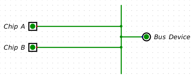
Enter the so called open drain or open collector. What this means is really simple, an chip with open collector/drain outputs can’t provide power (+5v) by itself, it can only provide an 0 (ground). Let us illustrate a simple circuit:

Picture above has two chips connected to one bus, and both chips are set o 0 (ground) which is no problem. But what would happen if Chip A would put out an 1 and Chip B an 0 (ground)?
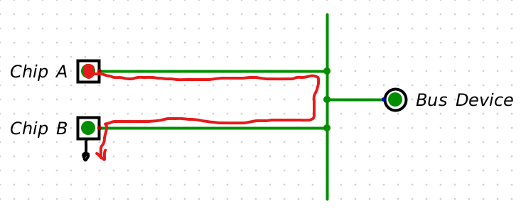
Bad thing right? So if we now assume that our chips have open drain outputs what would happen if Chip A was set to 1?
Well nothing, as an open drain can’provide power by it self, so even if the chip internally is set to 1, there is no power coming to the chip. So how do we represent an 1 then? The simple answer is, by adding power to the bus, but through an resistor so that we do not have an short circuit.
Enter the pullup resistor
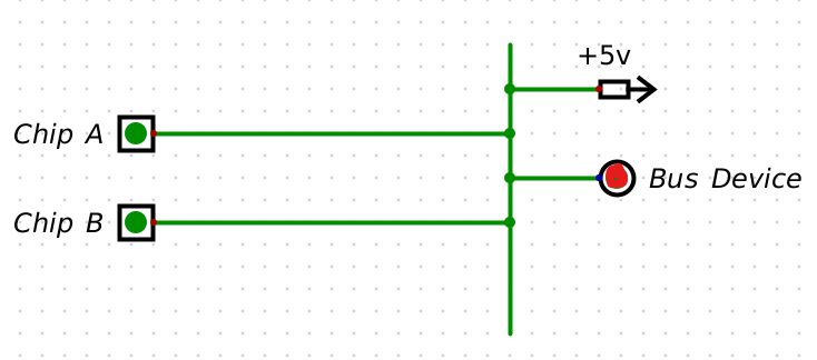
What we have added is an resistor from the bus to +5v and the bus device is now at an 1. If one of Chip A and B (let assume Chip A) asserts an 0 (ground), current will flow from +5v through Chip A to ground, but this time through an resistor, and therefore Bus Device will recive an 0 (0v) and without an short circuit.
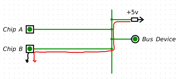
A common word for this is to “sink current” and is based on least resistance. Selecting size of resistor is done by not cause an voltage drop over the resistor so large, that the voltage on the input pin goes below the HIGH threshold.
Another thing that an pullup(or pulldown) resistor is used for is to ensure that there is an known state on an input, either low or high. Unconnected pins (known as floating) can act erratic as they cant detect it it should be a logic high or low.
Tri-State
So, if we have an chip sitting within our circuit, and we have an active low CE-signal that we set high, what happens? As we have seen above, depending on chip, we get different results. In data buses, where we would like to have one device at an time accessing the bus, we need to ensure that we do not have chips on the bus that take default state to ground (0) as it will (if not causing an short circuit!) interfere with anything talking to the bus. An tri-state chip acts as it was not connected at all when it’s not enabled. This functionality is called Tri-state or high impedence, and are very common on buffers or bus trancievers. The Motorola CPU itself have Tri-state pins, ensuring that the buses ar completely disconnected when for example an bus error are triggered, address cycle is not active, or an device on the bus have asked the CPU for ownership (called bus mastering, and and an topic for later days) . Tri-state is another way of solving the issues that before was solved by open drain, but as you will se in our project there are use cases, even today, where open drain is the preffered (and neccessary due to known state as mentioned above) method
Other uses of pull up / pull down
Now, there are other use cases for using pull up / pull down resistors. One of the more important ones, especially on buses, is the fact that copper traces /wires acts as antennas. Having a bus just floating could cause interference, and are the traces or cables long enough, it could start generate erratic behaviours, causing chips to interpret signals as high or low. So, for that reason, I prefer to pull things to ground or VCC. This however causes you to take timing into account, as pulling something from one state to another will take longer, and you also need to consider resistor load to ensure that an chip can overcome the pull up / pulldown resistance