So we are ready to start connecting ROM and RAM to the CPU, but before we do this, we will have an look at the address bus of the MC68010
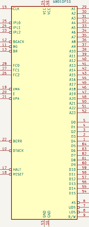
Wait, there is only 23 address lines? This must mean that the CPU can only address 8 MB of RAM and not 16?
Well, the people at Motorola did it in an way that confused me quite a bit to start with, but when the penny dropped, it’s quite straight forward. The CPU have two additional outputs called UDS and LDS. Before explaining this, lets dig into some stuff.
Endianness. Say what?
Wikipedia have an good article on this, but to simplify stuff, there are two ways to store data in memory, Big-endian, and Little-endian. To illustrate this, let us draw an table to represent the longword data (4 bytes) to be read from ROM at first address (0x00000000) when the CPU startup to load the stack pointer address value. Every address store one byte (8 bits of data). In this example we have set the stackpointer address value to 0x00208040 :
| 0x00000000 | 0x00000001 | 0x00000002 | 0x00000003 |
|---|---|---|---|
| 00 | 20 | 80 | 40 |
A big-endian system stores the most significant byte (8 bits) of a word (16 bits) at the smallest memory address and the least significant byte at the largest.
A little-endian system stores the least significant byte (8 bits) of a word (16 bits) at the smallest memory address and the most significant byte at the largest.
For those new to most/least significant byte: The leftmost (first) byte is the most significant (containing the most significant eight bits of the corresponding bit string), and the rightmost (last) byte is the least significant (containing the least significant eight bits of the corresponding bit string).
The MC68010 have an 16 bit data bus, that can be read/written either by 8 bits (byte) or 16 bits(word). As we can se from the table containing two words (longword), the Motorola architechture is an big-endian one, as the most significant bit is at the lowest address. Using this example, if one would like to read the lower byte (least significant) of the second word (two bytes), one should look at address 0x00000003. And if you would read the upper byte (most significant byte) of the same word, you would look at address 0x00000002, which is the lowest address in that word. As you can see, the upper byte address is always an even number, and the lower address is always an odd number, and often referenced in this way. We will hit that nomenclature when connecting stuff to the CPU.
UDS and LDS – how to cherrypick your bytes
So, back to the fact that the CPU only have 23 address lines and the mention of the pins LDS and UDS. LDS stands for Lower Data Strobe, which means that when this pin is active low, (0), the lower (odd), byte is requested. And then as you might expect, UDS means Upper Data Strobe and that the upper (even) byte is requested. If an full word (16-bit) is requested, both UDS and LDS will be asserted low (0) and the whole word will be accessed in one go.
By using this scheme, Motorola made it simple to pull a single byte (and in effect isolate a byte on the bus, but that we will cover later) instead of always pulling two bytes of the 16-bit data bus and in code select upper or lower byte of the word.
Extending the address bus
Now let us exemplify using the table above. In code we pretend that we would like to read a byte of data from adress 0x00000000. This means that all 23 address pins on the CPU is set to low (0), and the UDS (since 0 is even (well…mathematically at least) is set to active low (0), whereas LDS is set to high (1).
But what if we would like to read the next byte at adress 0x00000001? Well, when our code asserts address 0x00000001, all 23 address lines are once again set to low (0), but the LDS is set to active low (0) and UDS is set to high (1).
What we se here is the fact that reads of two addresses had the same state of the address bus pins, and selecting address was done by the UDS and LDS pins, in effect giving us an additional address pin, as we now can select two byte per pin.
Finally, if we in code assert that we would like to read a whole word (both upper/even and lower/odd) at once, the CPU will assert both UDS and LDS to active low(0).
Implications to be aware of in this architecture
Now, a consequence of this architecture have an impact on how you write code for the CPU, and the word for it is alignment, which we will run into when we start to create code.
One simple rule: Any reads or writes that are larger than a byte must start at an even address! Once again let us use the table above as an example. What would happen if your code is asking to read a word (2 bytes) starting at address 0x00000001?
The CPU will try to set all address lines to low (0) just as when addressing 0x00000001 when reading as an byte and assering LDS active low(0). But since you have asked for an word (two bytes), the next byte is actually only avaliable if address line one(1) is set to active (1). Remember from the example above that an word on the bus is based on that the address line are in the same state, and handled by UDS and LDS. So we have a conflict of addresses that will cause the CPU to fire an exception.
I repeat, One simple rule: Any reads or writes that are larger than a byte must start at an even address! This limitation is removed in the MC68020/30/40/60 CPUs, but requesting unaligned data in those CPUs have an severe penality in performance, so I say it again: Any reads or writes that are larger than a byte must start at an even address!
Clear on that? 🙂
Types of ROM and RAM
In my design I use 512 Kb of ROMs and 512Kb of RAM chips. Why is that? And what ROMs and RAMS can I use? And why two and not one?
Well, there is a bunch of things here that can make your design go one way or another. First off, I would like to mention that there are two types of RAM (in general) to choose from: Static RAM (SRAM) and Dynamic RAM (DRAM). Also, speed of the chips is an factor. This we will skip for later. The difference is twofold:
– Price: SRAM is more expensive, but simpler to implement
– Complexity: DRAM needs additional circuitry, SRAM don’t
The reason for DRAM beeing the most used RAM of today in consumer product is price. Even if there are additional circuits needed for DRAM, the total cost is lower than SRAM.
However, in my design, I use SRAM, as it simplify the design, and makes life easier.
The next thing to consider is how we access data. In our case, we have an 16-bit data bus, but would like to access data at an byte level. RAM comes in different shapes and forms, and the nomenclature is usualy like: 64k x 8 where the first number is the number of addresses, and the second the width of the data output from the chip. This means that the ram has ~64000 blocks of eight bit data. In effect an 64 Kb (kilobyte) of memory. Another example is 1M x 16 which means that you have ~1000000000 blocks of 16 bit data, in effect 2MB (megabyte) of memory. There is also as an example 64k x 1, which in effect means that you have 8Kb (kilobyte) of memory
Also, as we showed above, each byte in an word is accesses depending on The UDS and LDS pins beeing active low(0), so in principal the easiest way is to have one RAM chip with eight databits (for example 64k x 8) connected to the upper/even byte, and one RAM chip connected to lower/odd byte. Now there are other ways to do this. You could have eight 64k x 1 chips connected at each dataline (quite common back in the early days of home computing) that would result in alot of chips. Trying to use chips with bigger data bus than byte size (lets us say 1M x 16) would require additional circuitry involving LDS/UDS pins even if it is possible in theory. So to keep it simple, I use 512K x 8, one connected to the upper/even data lines (8-15), and one to the lower/odd data lines. Both chips connects their address lines to the same address pins and we will use some decoding logic to select either upper/even or lower/odd.